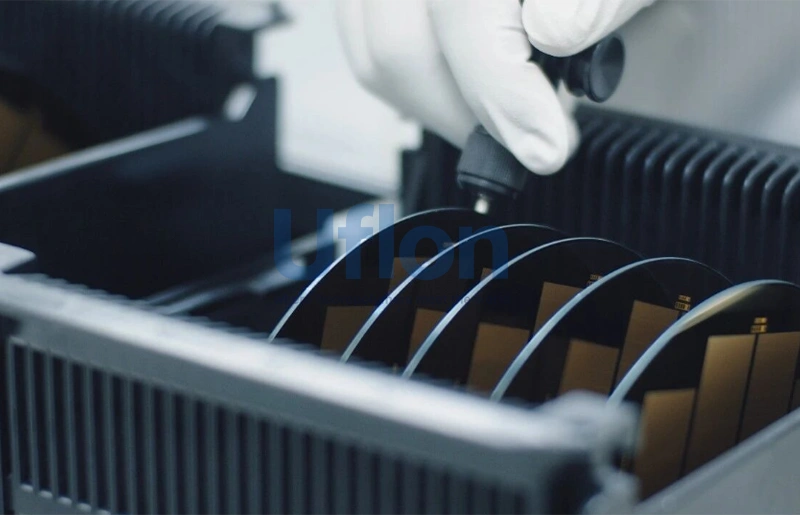
Against the continuously improved requirements of advanced semiconductor processes, the market evaluation criteria for semiconductor carrier materials has upgraded accordingly. Do not only meeting basic properties such as temperature resistance and antistatic performance, dimensional stability, low precipitation, uniform surface resistivity and batch consistency are gradually becoming important indicators.
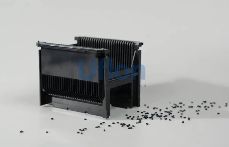
PEEK, as a material for wafer carrier, it plays an indispensable role in semiconductor applications.
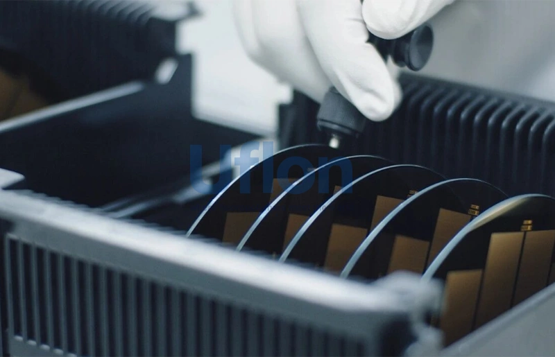
Over the past two years, customers have attached great importance to "resistivity stability" and "consistency of injection moulding appearance". We have continuously optimized material performance. Today, our PEEK material can deliver superior surface appearance, higher uniformity of surface resistivity across all faces, stable antistatic performance and no flow marks.
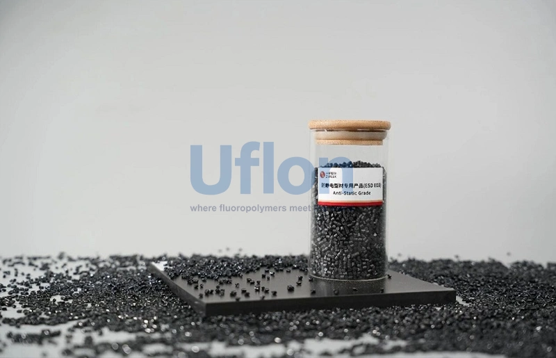
Continuous iteration and optimization of PEEK material focus on resolving four key aspects:
1. Resistivity Stability
Rely on its semi-crystalline structure and rigid molecular chains, together with homogenous filler modification and low-internal-stress moulding processes, our PEEK achieves low shrinkage and low anisotropy.
It maintains stable dimension and carrier accuracy during high-low temperature cycling as well as wafer storage and transportation.
2. Low precipitation and cleanliness
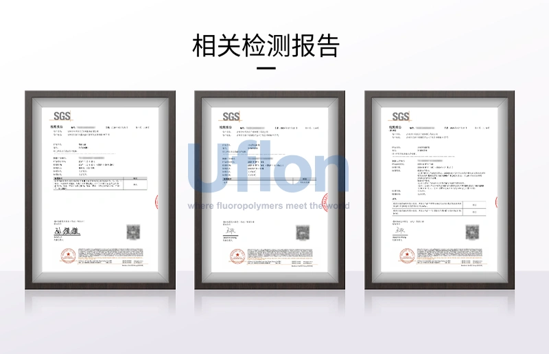
Passed the RoHS, REACH, metal ion,and surface positive/negative ion tests.
PEEK has low degassing and low hygroscopicity properties, combined with modification process, it can be well adapted to application scenarios with high requirements for gas cleanliness and ion cleanliness.
3. Antistatic uniformity
PEEK matrix are evenly dispersed conductive fillers to form a continuous conductive network.
This prevent local static charge accumulation, matching the cleanliness and electrostatic protection requirements in semiconductor manufacturing processes.
4. Wear resistance and cleanliness
Our carbon fiber reinforced series of PEEK offers excellent wear resistance. Under the relevant test conditions, after multiple loading and unloading cycles, the contact surface still maintains a good surface condition, preventing scratches on the wafer's backside or introducing particle contamination.
100 meters northwest of Changiiafang Village Committee, Gaoging County, Zibo City, ShandongProvince
Copyright © 2025 by Zibo Uflon New Material Technology Co., Ltd. All Rights Reserveds
Privacy Policy